Gameboy Development Forum
Discussion about software development for the old-school Gameboys, ranging from the "Gray brick" to Gameboy Color
(Launched in 2008)
You are not logged in.
Ads
#1 2018-04-24 15:43:25
- endrift
- Member

- Registered: 2017-05-24
- Posts: 16
MBC6 research
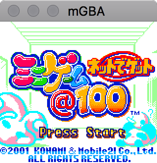
Researching Net de Get: Minigame @ 100 cartridge (the only MBC6 game)
Register descriptions:
0x0000: Standard SRAM access control (0/A, etc)
0x0400: SRAM bank 0 control (0xA000-0xAFFF, 0x1000 bytes per bank, 8 banks total)
0x0800: SRAM bank 1 control (0xB000-0xBFFF, 0x1000 bytes per bank, 8 banks total)
0x0C00: Output enable (?)
- 00: Disabled
- 01: Enable reading/writing to chip (via standard commands)
0x1000: Write enable
- 00: Disabled
- 01: Enable writing to 0x0C00 and programming the chip
0x2000: ROM bank 0 bank ID (0x4000-0x5FFF, wraps, 0 can be mapped in freely, setting top bit seems to unmap ROM)
0x2800: ROM bank 0 bank type (0 = ROM, 8 = flash, other bits unknown)
0x3000: ROM bank 1 bank ID (0x6000-0x7FFF, wraps, 0 can be mapped in freely, setting top bit seems to unmap ROM)
0x3800: ROM bank 1 bank type (0 = ROM, 8 = flash, other bits unknown)
Uses standard flash commands with addresses 2:5555 (store AA) and 1:4AAA (store 55) (bank 0) / 2:7555 (store AA) and 1:6AAA (store 55) (bank 1)
Simple code for getting JEDEC mfg/dev IDs (C2/81):
Code:
    ld a, 1
    ld [$1000], a ; Turn on write enable
    ld [$0c00], a ; Turn on output enable
    xor a
    ld [$1000], a ; Turn off write enable
    ld a, 2
    ld [$3000], a ; Map physical bank 2 into bank 1 address space
    ld a, 8
    ld [$3800], a ; Map flash
    ld a, $AA
    ld [$7555], a ; Write AA to 2:7555 (flash handshake)
    ld a, 1
    ld [$3000], a ; Map physical bank 1 into bank 1 address space
    ld a, $55
    ld [$6AAA], a ; Write 55 to 1:6AAA (flash handshake)
    ld a, 2
    ld [$3000], a ; Map physical bank 2 into bank 1 address space
    ld a, $90
    ld [$7555], a ; Write 90 to 2:7555 (JEDEC ID mode)
    ld a, 0
    ld [$3000], a ; Map physical bank 0 into bank 1 address space
    ld a, [$6000] ; Load JEDEC manufacturer ID (C2, Macronix)
    ld a, [$6001] ; Load JEDEC device ID (81, MX29F008TC-14)
Just implementing RAM/ROM bank switching is enough to make the game playable.
Programming the chip is done by first erasing a sector:
Code:
0:1000 := $01 ; Enable writing
2:7555 := $AA
1:6AAA := $55
2:7555 := $80
2:7555 := $AA
1:6AAA := $55
X:X000 := $30 ; Sector erase command
WAIT FOR [X:X000] = $80
where X:X000 corresponds to the bank/address of the sector (4kB size). Read out any address in the sector until it equals 0x80 before continuing. This is the signal that it's done erasing.
This resets the entire 4kB sector to 0xFF.
Then you can write to the chip in 0x80-byte blocks, followed by writing a $00 byte on the last address and reading until it's 0x80, followed by issuing command 0xF0 to exit program mode and disabling write enable, e.g.
Code:
0:1000 := $01 ; Enable writing
0:0C00 := $00 ; Enable output
0:1000 := $00 ; / Unclear if this part is necessary
0:1000 := $01 ; \ Net de Get does it though
2:7555 := $AA
1:6AAA := $55
2:7555 := $A0 ; Program command
X:X000 := $XX
...
X:X07F := $XX
X:X07F := $00 ; Unclear if this write is necessary, Net de Get does it though
WAIT FOR [X:X07F] = $80
2:7555 := $AA
1:6AAA := $55
2:7555 := $A0
X:X080 := $XX
...
X:X0FF := $XX
X:X0FF := $00
WAIT FOR [X:X0FF] = $80
...
2:7555 := $AA
1:6AAA := $55
2:7555 := $A0
X:XF80 := $XX
...
X:XFFF := $XX
X:XFFF := $00
WAIT FOR [X:XFFF] = $80
2:7555 := $AA
1:6AAA := $55
2:7555 := $F0 ; Exit program mode
0:1000 := $00 ; Disable writing
Note that writing can only set bits to 0; erasing first is necessary to bring the bits back to 1.
Last edited by nitro2k01 (2019-09-01 19:34:53)
Offline
#2 2020-09-04 02:50:45
- endrift
- Member

- Registered: 2017-05-24
- Posts: 16
Re: MBC6 research
So a bit of an update on this, after I asked nitro to remove the "WIP" from the subject: the game writes 0xC6 to the bank type registers and I have not yet figured out why yet.
Offline