Gameboy Development Forum
Discussion about software development for the old-school Gameboys, ranging from the "Gray brick" to Gameboy Color
(Launched in 2008)
You are not logged in.
Ads
#1 2010-03-08 03:17:50
- Echelon_Force
- Member

- Registered: 2010-03-08
- Posts: 11
- Website
LCD Board Help? (ribbon cable pinout and functions)
I'm trying to identify and spec out the LCD signals in the GB (classic). I'm looking to do away w/ the GBs original controller board while keeping the LCD board.
Basically I want to plug the ribbon cable into my on PCB and output the necessary signals to drive the video myself.
I'm just wandering if anyone has more info on LCD signals output by the z80 so I can emulate them to display stuff.
So far I've mapped all the buttons, speaker, power LED, LCD negative power to the appropriate pins on the ribbon cable.
What I have so far:
Note: Pin 01 is the pin on the ribbon cable closest to the power switch (at the cables connector).
Note: Pin LCDV1 is the pin closest to power switch on the LCDs vertical axis connector (beneath LCD).
Note: Pin LCDH1 is the pin closest to power switch on the LCDs horizontal axis connector.
Pin 01 GND
Pin 02 Power LED - (Unregulated Batteries Voltage)
Pin 03 LCD Drive voltage (-19 V) This voltage comes from the voltage converter attached to the CPU section.
Pin 04 Left & B buttons
Pin 05 Button Diodes 1 & 2
Pin 06 Down & Start buttons
Pin 07 Up & Select buttons
Pin 08 Right & A Buttons
Pin 09 Button Diodes 3 & 4
Pin 10 GND
Pin 11 Vcc - Regulated 5V (different from Pin 02).
Pin 12 VERTSYN (I think) Goes to LCDV8.
Pin 13 ? - Connects to LCDV6 and LCDH7 (Either DATALCH or ALTSIGL)
Pin 14 CLK ? - According to nitro2k01's inverted display mod. Connects to LCDH8. (Data suggests Pin 18 as CLK though.)
Pin 15 DATAOUT1 ? - According to nitro2k01's inverted display mod. Connects to LCDH9.
Pin 16 DATAOUT0 ? - According to nitro2k01's inverted display mod. Connects to LCDH10.
Pin 17 ? - Connects to LCDH11 (Either CONTROL or HORSYNC)
Pin 18 ? - Connects to LCDV10 and LCDH12 (Either DATALCH or ALTSIGL) (Data suggests Pin 18 as CLK but this conflicts with LCD schematic...)
Pin 19 ? - Connects to LCDH13.
Pin 20 Speaker
Pin 21 GND
So I need help assigning Pins 12-19. I also need to know exactly what they do, and whether the controller or the LCD driver chip(s) are the ones switching them.
Basically...the sequence in which to flip bits...
I do have the LCD section schematic from devrs.com (gameboy2.gif) but it doesn't have the ribbon pinout or explain what the non-obvious signals do.
Here's a bit of captured data from all those pins...my current setup doesn't really do time stamping, so it's virtually useless...unless you want to know that 3 frames fits in 7000 bytes:
Offline
#2 2010-03-08 06:23:01
- nitro2k01
- Administrator
- Registered: 2008-02-22
- Posts: 252
Re: LCD Board Help? (ribbon cable pinout and functions)
Check this image first: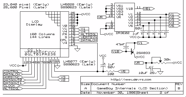
See also: http://gbdev.gg8.se/wiki/articles/DMG_Schematics
The buttons only need the 6 connections to work, not Gnd or anything else.
Also, your picture doesn't work...
Offline
#3 2010-03-08 11:02:00
- Echelon_Force
- Member

- Registered: 2010-03-08
- Posts: 11
- Website
Re: LCD Board Help? (ribbon cable pinout and functions)
I have those schematics (as I clearly stated in the first post!). They do not tell me what the signals do exactly.
I have tried the image in all my browsers and it does work... All the same it is available here too:
http://www.robotdialogs.com/
or here:
http://picasaweb.google.com/lh/photo/ur … directlink
I know the buttons don't need GND to work. I also could care less. They are mapped and the circuit is simple to understand. I am only concerned with mapping and understanding the purpose of Pins 12-19 on the ribbon cable.
Offline
#4 2010-03-08 12:39:02
- nitro2k01
- Administrator

- Registered: 2008-02-22
- Posts: 252
Re: LCD Board Help? (ribbon cable pinout and functions)
If you don't believe me... Here's what the image looks like for me (Firefox) which means that the image could not be loaded.
This is what it looks like when I try to copy/paste the URL into the address bar.
Maybe it works just for you since you are still logged in to Picasa?
Anyway, I got a little confused and didn't think you had that schematic because you didn't use the numbering in the schematic. Anyway, the pins marked as V1-V5 are likely voltage reference levels used for the 4 colors. As you can see, it is connected to the IR3E02 contrast control chip.
I may be wrong about what I called clock. I could tell from the waveform on the oscilloscope that it is a clock signal, not necessarily the one named CLOCK in the schematic. I'll take a wild guess and and say that CLOCK is probably the CPU clock, and that DATALTCH is the signal for latching a new value from the DATAOUT1 and DATAOUT2. DATALTCH probably goes at the same rate as CLOCK, but is only active when the display is receiving data. I don't know exactly how VERTSYNC and HORSYNC look, but they're obviously related to the vertical and horizontal blanking. Wild guess again, they low during their respective blanking period and high during the active period when data is transferred. (Or the other way around)
I don't have a clue what CONTROL does, but it might be the master on/off switch when the GB requests the display to be turned off for power saving. ALTSIGL, no clue there either.
I'll try to find the information or experiment to see if I can figure it out. I know a few people who might know. You could try to cut the lines you don't know what they do and see what it changes. But if you do that, and the LCD doesn't get a picture, turn off the power or you might get permanent LCD damage.
Offline
#5 2010-03-08 14:09:00
- Echelon_Force
- Member

- Registered: 2010-03-08
- Posts: 11
- Website
Re: LCD Board Help? (ribbon cable pinout and functions)
I have no idea what the problem is with the image...I can load it fine from each PC I try (logged in and not)....oh well...do the other links work?
I think your probably correct on the CLOCK and DATALTCH signals. CONTROL and ALTSIG are the real head scratchers...it's too bad the guy who named them in that schematic did it 20 years ago. :)
I'm going to work on an improved data collection method tonight to see if I can get time stamped data. Currently I have an AVR uC patched into those 8 signals and I can record a few full frames before filling its memory...
Once I've collected what I can from that I'll solder into both the cable (done already) and its connector. That way I wont need to cut anything, and if necessary I can do a man-in-the-middle analysis with the uC.
Do you think it might be possible that the LCD is driving ALTSIGL? I'll be able to tell for sure when I get in the middle of the cable...it just seems that there should be some kind of feedback from the LCD...I've never worked with them before at this low level so I just don't know.
Offline
#6 2010-03-10 02:21:00
- Echelon_Force
- Member

- Registered: 2010-03-08
- Posts: 11
- Website
Re: LCD Board Help? (ribbon cable pinout and functions)
Well I managed to finish patching into the connector side of the ribbon cable. I've determined that Pin 13 doesn't do anything at all (at least in the boot w/o cart). If it's removed the video displays just fine. (This still could have something to do with the different LCD modes available in GB assembly code, but I probably wont investigate this.)
All the other pins (12, 14-19) are essential for video.
Pins 15 and 16 I think I can confirm as being the data lines though I can't confirm which is which. The video gets darker if one either is removed...thus more zeroes are sent to the LCD...
I'm also pretty now that 18 is the main clock...it's the only thing that always toggles.
I've also made progress toward getting a uC in the middle of the cable. Unfortunately I can't get the uC's clock speed high enough to allow even a straight pass through. With the GB operating at ~4MHz I thought 8MHz would be sufficient to allow pass through, but even at 11.0592 MHz (fastest oscillator crystal I have) there is distortion of the video. This result tells me several things.
1. My data captured before is completely useless because insufficient clock speed means i can even replicate/record the clock from the GB.
2. I'm at a stand still with the man-in-the-middle process until I can increase clock speed or get a faster data collection device (probably going to purchase this: http://dangerousprototypes.com/2010/02/ … nalyzer-2/ for the task).
3. My only option at this point is to take an educated guess at the remaining 4 signals base on the schematics and mapping I did and what inaccurate data I collected and attempt to trial and error my way to a working display. This could take forever to get correct.
I'm more likely to wait and do option 2 unless someone else can capture some accurate data and shoot it my way.
FYI my code for passing data straight through was essentially:
for(;;){
PORTA=PINC;
}
I might be able to get faster results w/ assembly but I wouldn't be able to do serious analysis in assembly.
Offline
#7 2010-03-10 08:48:24
- nitro2k01
- Administrator

- Registered: 2008-02-22
- Posts: 252
Re: LCD Board Help? (ribbon cable pinout and functions)
On AVR, read I/O and write I/O are 1 cycle each, and a short branch is 2 cycles, (I'm assuming here that the compiler knows how to optimize the code properly) so just to forward the signal and avoid distortion you need a frequency of at least 2 times the GB clock, and that's only if the 2* clock is synchronized with the GB clock. If it isn't you'll get overlap and still get distortion on at least some pixels. To process the data you need to go a lot higher. This is under the assumption that the video clock is running at half the rate of the system clock. Since 160*144*60=1382400 and the clock is silent during the blanking periods, this is a fair assumption.
Furthermore, all GB's are using a nonstandard clock based on powers of two. Instead of 4 MHz, it actually runs at 4 MiHz, or close to 2^22 Hz. Thus, regular 1.00000 MHz multiple crystals will be out of phase with the GB. One way to solve this could be to actually clock the GB from the uC.
A better option would be to use some sort of programmable logic, eg an FPGA.
Also, I suggest you drop by the IRC channel #gbdev on EFNet to discuss this with more people.
Offline
#8 2010-03-10 11:27:51
- Echelon_Force
- Member

- Registered: 2010-03-08
- Posts: 11
- Website
Re: LCD Board Help? (ribbon cable pinout and functions)
I'm a big fan of the clocking the GB from the uC idea. I might try that this evening if I can figure out a (somewhat) non-destructive way to do it. I'll have to take a closer look at the main board.
If all else fails I'll order that logic sniffer/analyzer which will have plenty of speed.
I'll hop on that IRC channel next time I get a chance.
Offline
#9 2010-03-10 11:56:26
- nitro2k01
- Administrator

- Registered: 2008-02-22
- Posts: 252
Re: LCD Board Help? (ribbon cable pinout and functions)
To clock the GB you need to remove the crystal. The top pin (the one nearer the top of the board) can be used as a clock input. You should also probably try to avoid not sending the a clock signal for too long. (Might possibly damage the LCD if it doesn't get updated regularly.)
Offline
#10 2010-03-10 12:30:57
- Echelon_Force
- Member

- Registered: 2010-03-08
- Posts: 11
- Website
Re: LCD Board Help? (ribbon cable pinout and functions)
Thanks, I've been scouring the web to figure out which pin to use. I'm not sure how slow I'll have to make it... I'll probably set it up so that I clock it at near normal speed and then reduce it until I start to have issues...This particular LCD has taken quite a bit of abuse and still works, so I'm not terribly worried about slowing it down...
Also I plan to clock it using the PWM/timer hardware in the AVR so it shouldn't be difficult to get a steady clock speed and still have all the AVR CPU cycles to analyze with...
Offline
#11 2010-03-25 03:37:42
- Echelon_Force
- Member

- Registered: 2010-03-08
- Posts: 11
- Website
Re: LCD Board Help? (ribbon cable pinout and functions)
Minor Update with a bunch of pictures: http://www.robotdialogs.com/2010/03/gam … art-2.html
Offline
#12 2010-07-24 13:47:21
- Echelon_Force
- Member

- Registered: 2010-03-08
- Posts: 11
- Website
Re: LCD Board Help? (ribbon cable pinout and functions)
So i've ordered a logic analyzer. I will be posting on this front again soon.
Offline
#13 2010-07-25 09:35:29
- c_rpg
- New member
- Registered: 2010-07-25
- Posts: 4
Re: LCD Board Help? (ribbon cable pinout and functions)
I've done some measurements as well. It was on a Super Gameboy, but they should be about the same. I only have a regular scope, so I could only take arbitrary measurements.
Here is the horizontal sync line with one of the data lines. 18 bytes are sent to form a complete line (144 pixels).
Here is the clock line with one of the data lines. There are 8 bits per clock cycle.
Something interesting is that if you connect both data lines to eachother, you get a picture but only the lightest and darkest color are shown. This is correct because you are creating some form of AND gate effect. The signals both go to low (0V) if one of the lines is low. The signals can only be high if both signals are high (1).
So the truth table is like this:
|shade1|shade2|shade3|shade4|
DATAOUT0 | 0 | 1 | 0 | 1 |
DATAOUT1 | 0 | 0 | 1 | 1 |

VSYNC and HSYNC. Logically there should be 160 HSYNC pulses per VSYNC cycle.
Sorry for the crappy quality on the pictures.
Last edited by c_rpg (2010-07-25 12:08:07)
Offline
#14 2010-07-25 23:48:22
- Badut
- New member
- Registered: 2010-07-25
- Posts: 1
Re: LCD Board Help? (ribbon cable pinout and functions)
That's nice info c_rpg.
Question about the clock versus data line image.
I'm assuming trace 1 is clock and trace 2 is the data? is that correct?
This would make sense as the clock would be a somewhat regular square wave while the data can go high/low anytime.
What would be really useful if you (or anyone else reading this) had the time to post scope traces of some of the other signals. Sadly, I don't have a scope so I need to beg someone to do this for me.
My own measurements/experiments with a multimeter lead to the following educated guesses:
ALTSIGL is related to HORSYNC somehow. It looks like ALTSIGL toggles every HORSYNC (ie. ALTSIGL is high for every second row of pixels)? In other words, its frequency is half of HORSYNC. Don't know enough about LCD's to think of why this is necessary. Would be nice to confirm this.
DATALCH is not "data latch" if my measurements are worth anything. Its frequency is too slow to be latching data. It appears to go high roughly as often as HORSYNC.
I know shorting this to GND causes the LCD to draw a single black horizontal line across the screen. The position of the line is random. It's almost like this signal is some sort of carriage return. Again I think a CRO trace of this against HORSYNC would reveal something useful.
CONTROL I have no idea. But it's important - disconnecting it causes no image to appear on the LCD. Looks like CONTROL is high at least a few times each scanline. A trace of this next to HORSYNC might give a clue what it does?
Offline
#15 2010-07-25 23:56:33
- Echelon_Force
- Member

- Registered: 2010-03-08
- Posts: 11
- Website
Re: LCD Board Help? (ribbon cable pinout and functions)
I second everything Badut has requested. I will be getting a logic analyzer soon (waiting on shipping from china) that'll do all 8 signals at once. With that I hope to capture a full frame of data or at least the beginning and end of a frame so we can finally unravel what all of the control signals do. The data and vert/horz syncs are fairly straight forward...
I think in c_rpg's second screen shot it's clk on top and data on bottom...it doesn't make sense the other way around.
Offline
#16 2010-07-26 13:04:29
- c_rpg
- New member
- Registered: 2010-07-25
- Posts: 4
Re: LCD Board Help? (ribbon cable pinout and functions)
I'm not sure what the data and clock lines are. But I think the top one was not clock. I just followed Jeff Frohwein's schematic of the super gameboy, but it doesn't seem to be 100% correct, nor is it complete.
I'm unable to double check the signals or take any extra measurements at the moment but I might check it out again during the weekend. The ICD2-R chip has already been desoldered on my super gameboy, but the cpu should still deliver the same signals. I'm not sure if it will boot however, with the chip removed.
Offline
#17 2010-08-05 01:19:15
- Echelon_Force
- Member

- Registered: 2010-03-08
- Posts: 11
- Website
Re: LCD Board Help? (ribbon cable pinout and functions)
I've finally acquired the logic analyzer and made a post with new data. Will be attempting to get working code this weekend.
http://www.robotdialogs.com/2010/08/gam … art-3.html
Offline
#18 2010-08-05 18:53:50
- c_rpg
- New member
- Registered: 2010-07-25
- Posts: 4
Re: LCD Board Help? (ribbon cable pinout and functions)
Ok I'll just dump some information here that I've collected. It's just bits and pieces, but it might come in handy to understand the signals. It's very confusing because Nintendo used different names for the signals. Also Sharp themselves have different names for one signal.
First of all the ALTSIGL pin:
Aliases: FR (used for common driver), M (used for segment driver), Alternate Signal, LCD Driver Clock, Liquid Crystal Drive waveform AC conversion signal input...
This is a table I took from one of the datasheets (LH5006A). It (probably) won't be completely the same as the Gameboy driver, but the function is similar.
This signal basically determines what the output voltage for the liquid crystal drive is.
Control or /DISPOFF: this input is used for the output drivers along with the ALTSIGL input. It determines what the output level of the drive is.
The voltage level of the out put pins (Y0,Y1,Y2,...) can be altered by:
1) changing the voltage level at V0-V5
2) using the ALTSIGL and control pins according to the truth table
You could make a truth table like this:
ALTSIGL|CONTROL=0|CONTROL=1|
0 | V? | V? |
1 | V? | V? |
I don't know what driver input voltage corresponds to which control inputs, but you get the picture. It's basically some kind of switch (or analog multiplexer) that selects the driver voltage according to two logic inputs.
Figuring out which pin corresponds to which signal is not easy, but I think the ALTSIGL is signal 7 and Control is signal 1. It would also make sense that these two lines are used to select the driver voltage because they are not connected in the super gameboy. The super gameboy does not need these signals to display the data on a television.
______________________________________________________________________________________________________________________________________________________________________________________
Next is the latch input. The datasheets use two latch inputs: the data latch and the line latch. The data latch is the signal which latch the blocks (which can be 4,8,16,... bits depending on the driver) into the shift registers.
The line latch will latch an entire line (in our case 160 bits) to the output pins.
Both latch lines should work on high->low transitions according to the datasheets.
The signals you captured shows aprox. 160 clock pulses (assuming signal 2 is clock) per block. Signal 6 might be the data latch because it has a high->low transition after every block. So this would result into a 160bit block.
This could mean there is only 1 latch input. Which should be set from high to low after each block.
______________________________________________________________________________________________________________________________________________________________________________________
The clock line is used to shift the data into the internal registers . Data is read at every falling edge.
______________________________________________________________________________________________________________________________________________________________________________________
I have finished the pcb design for the super gameboy IC in eagle but allas I haven't been able to etch a pcb yet. I have to work 4 more days and than I should have more time...
Last edited by c_rpg (2010-08-05 19:59:12)
Offline
#19 2010-09-08 12:56:45
- c_rpg
- New member
- Registered: 2010-07-25
- Posts: 4
Re: LCD Board Help? (ribbon cable pinout and functions)
Just saying I'm still trying to figure this out. I've been busy with other projects and kind off neglected this.
I've finally etched te PCB though. It's far from perfect, but I should be able to get a working board within the next few weeks.
Once the PCB is done, I'll try playing with the various signals a little and maybe get some more insight.
Offline
#20 2011-01-21 10:52:20
- Pallas
- New member
- Registered: 2011-01-21
- Posts: 1
Re: LCD Board Help? (ribbon cable pinout and functions)
Hi all,
I wondered if someone is still trying to discover more about the GB lcd display. I have been trying for the last week to control the display from an arduino;
I figured since the lcd display IC is based on asynchronous logic it could easily be controlled by a slower microcontroller. So after getting some info from the people who have succeeded to reconstruct an image from the signal sent to the lcd display, I hooked up de display to the arduino board, I used the original dc-dc booster circuit for the minus 20 volts for lcd drive; hooked it up to the 5V supplied by the arduino board. The lcd +5V vcc is also supplied by the board, it would be unnecessary to get the 5V also from the booster; the booster doesn't need to be loaded and the board also delivers a very clean and stable+5V. After thinking a bit about the way the display is controlled I just connected vsync, hsync, both data lines and the clock line to the microcontroller and banged some code in it.. It is supposed just to scan the display and set all pixels to black for the moment.
I actually hoped it would work right out of the box but it doesn't; I see just a few black horizontal lines now and then.. Suppose Murphy's law is correct..
But where I am stuck at the moment is: do I need to do something with the data latch and/or altsignal/control lines? I just know too few about graphical LCD displays to guess what they are for.
Does anyone have a good suggestion?
The actual code loop (I think it is correct) in C:
if(horizontal>=143)
{
if(ledStat==0){
digitalWrite(led, HIGH);
ledStat=1;}
else{
digitalWrite(led, LOW);
ledStat=0;}
horizontal=0;
digitalWrite(vSync, HIGH);
}
if(clockcntr>=159)
{
clockcntr=0;
horizontal++;
digitalWrite(hSync, HIGH);
}
clockcntr++;
if(horizontal!=0){
digitalWrite(clock, HIGH);
digitalWrite(clock, LOW);}
digitalWrite(hSync, LOW);
digitalWrite(vSync, LOW);
The microcontroller manages to get about 6 complete display frames out in a second; it is a factor 10 less compared to the original GB display controller.. but it should work, doesn't it?
Update: thanks to excellent support on the IRC channel I got the info I missed:
one needs to alternate the ALTSIG signal per frame and the DATALATCH needs to be pulsed once AFTER every line of pixels..
might give it a shot this weekend, will post my progress in this thread.
Last edited by Pallas (2011-01-21 11:21:42)
Offline
#21 2011-02-26 18:12:22
- Echelon_Force
- Member

- Registered: 2010-03-08
- Posts: 11
- Website
Re: LCD Board Help? (ribbon cable pinout and functions)
Progress update.
http://www.robotdialogs.com/search/label/gameboy
Offline