Mitsubishi M64282FP
|
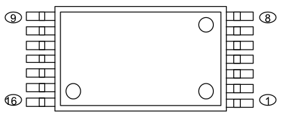
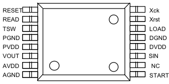
PIN CONFIGURATION (TOP VIEW) |
|
|
Outline : 16C 9-B |
Mitsubishi M64282FP, a.k.a the "Artificial Retina" is the CMOS image sensor used in the Gameboy Camera. Below follows the data sheet in wiki formatting; the data sheet is also available as a PDF in /docs/misc/ of the file hub.
Name: Mitsubishi Integrated Circuit M64282FP Image Sensor (Artificial Retina LSI) Version: ver. 1.1E Date: 5/21/98
Contents
Description
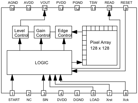
M64282FP is a 128 x 128 pixel CMOS image sensor with built-in image processing and analog image output tuning functions. This device can detect an image and process the image simultaneously as human retinas can. M64282FP can achieve smaller system size, lower power consumption, and more intelligent image processing functions.
Features
- Single 5.0V supply
- Low power dissipation ( Typ. 15 mW )
- Positive and negative image output
- Edge enhancement / extraction
- Output level & gain tuning
Application
Image input device, Gaming, Human interface for PC, etc
Block Diagram
Pin Configuration
| PinNo. | Symbol | Function | Description |
|---|---|---|---|
| 1 | START | Start Input | Image sensing start.
Pulled down internally by 10k ohm. |
| 2 | NC1 | Non Connect | |
| 3 | SIN | Data Input | Parameter input. Pulled down internally by 10k ohm. |
| 4 | DVDD | Digital Power Supply | Power for logic circuits. Must be connected to 5.0 V digital supply. |
| 5 | DGND | Digital GND | Ground for logic parts. |
| 6 | LOAD | Data Set Input | Parameter set enable. Pulled down internally by 10k ohm. |
| 7 | Xrst | System Reset | System reset terminal. Pulled up internally by 10k ohm. Low active. |
| 8 | Xck | System Clock Input | Clock input for MUX. Pulled down internally by 10k ohm. |
| 9 | RESET | Memory Reset Input | Parameter register reset. Pulled up internally by 10k ohm. Low active |
| 10 | READ | Read Image | Read image signal. |
| 11 | TSW | Reserved | NOTE: Don’t connect to this pin. |
| 12 | AGND1 | Analog GND | Ground for analog circuits. |
| 13 | AVDD1 | Analog Power Supply | Power for analog circuits. Must be connected to 5.0 V analog supply. |
| 14 | Vout | Signal Output | Analog image signal output in voltage. |
| 15 | AVDD2 | Analog Power Supply | Power for analog circuits. Must be connected to 5.0 V analog supply. |
| 16 | AGND2 | Analog GND | Ground for analog circuits. |
Image Sensing Specifications 1
| Item | Specification | |
|---|---|---|
| 1 | Resolution | 128 x 123 |
| 2 | Optical System | 1/4 inch |
Image Sensing Specifications 2
| Item | Specification | |
|---|---|---|
| 1 | Detectable Illumination Range (Faceplate) | 1 lx ~ 10000 lx [1] |
| 2 | Optical System | 1/4 inch |
| 3 | System Clock (Xck) | 500 KHz |
| 4 | Frame Rate | 10 fps ~ 30 fps |
| 5 | Output Voltage Range (Vout) | 2.0Vp-p |
Electrical Specifications - Absolute Maximum Ratings
| Symbol | Parameter | Limits | Unit | ||
|---|---|---|---|---|---|
| Min. | Typ. | Max. | |||
| DVDD | Digital Power Supply Voltage | 4.5 | 5.0 | 5.5 | V |
| AVDD | Analog Power Supply Voltage | 4.5 | 5.0 | 5.5 | V |
Electrical specifications - DC Specifications
| Symbol | Parameter | Limits | Unit | ||
|---|---|---|---|---|---|
| Min. | Typ. | Max. | |||
| VOH | "H" Output Voltage (READ) | 4.5 | DVDD | V | |
| VOL | "L" Output Voltage (READ) | 0.0 | 0.5 | V | |
| VIH | "H" Input Voltage | 2.2 | DVDD | V | |
| VOH | "L" Input Voltage | 0.0 | 0.8 | V | |
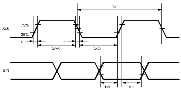
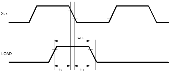
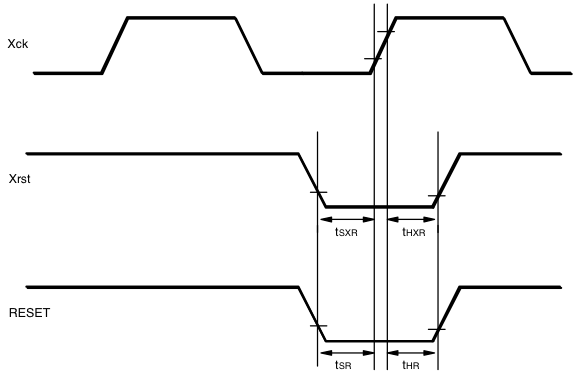
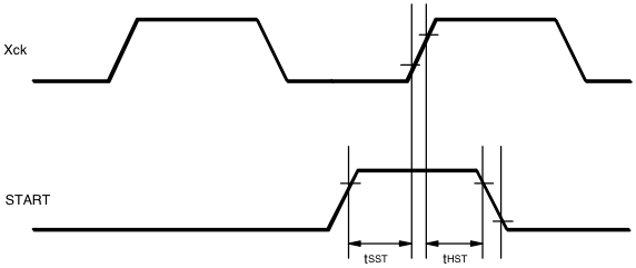
AC Timing Requirements
See the waveforms.
| Symbol | Parameter | Limits | Unit | ||
|---|---|---|---|---|---|
| Min. | Typ. | Max. | |||
| tcr | Xck cycle time | 2 | — | — | µs |
| tWHX | Xck high pulse width | 0.8 | — | — | µs |
| tWLX | Xck low pulse width | 0.8 | — | — | µs |
| tr | Xck rise time | — | — | 0.2 | µs |
| tf | Xck fall time | — | — | 0.2 | µs |
| tSS | SIN setup time | 0.4 | — | — | µs |
| tHS | SIN hold time | 0.4 | — | — | µs |
| tSL | SIN setup time | 0.4 | — | — | µs |
| tHL | SIN hold time | 0.4 | — | tWLX - 0.4 | µs |
| tWHL | LOAD high pulse width | 0.8 | — | — | µs |
| tSXR | Xrst setup time | 0.4 | — | — | µs |
| tHXR | Xrst hold time | 0.4 | — | — | µs |
| tSR | RESET setup time | 0.4 | — | — | µs |
| tHR | RESET hold time | 0.4 | — | — | µs |
