Mitsubishi M64282FP
|
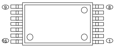
PIN CONFIGURATION (TOP VIEW) |
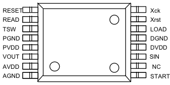
|
|
Outline : 16C 9-B |
Mitsubishi M64282FP, a.k.a the "Artificial Retina" is the CMOS image sensor used in the Gameboy Camera. Below follows the data sheet in wiki formatting; the data sheet is also available as a PDF in /docs/misc/ of the file hub.
Name: Mitsubishi Integrated Circuit M64282FP Image Sensor (Artificial Retina LSI) Version: ver. 1.1E Date: 5/21/98
Contents
Description
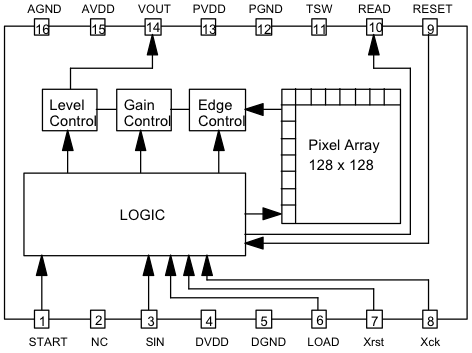
M64282FP is a 128 x 128 pixel CMOS image sensor with built-in image processing and analog image output tuning functions. This device can detect an image and process the image simultaneously as human retinas can. M64282FP can achieve smaller system size, lower power consumption, and more intelligent image processing functions.
Features
- Single 5.0V supply
- Low power dissipation ( Typ. 15 mW )
- Positive and negative image output
- Edge enhancement / extraction
- Output level & gain tuning
Application
Image input device, Gaming, Human interface for PC, etc
Block Diagram
Pin Configuration
| PinNo. | Symbol | Function | Description |
|---|---|---|---|
| 1 | START | Start Input | Image sensing start.
Pulled down internally by 10k ohm. |
| 2 | NC1 | Non Connect | |
| 3 | SIN | Data Input | Parameter input. Pulled down internally by 10k ohm. |
| 4 | DVDD | Digital Power Supply | Power for logic circuits. Must be connected to 5.0 V digital supply. |
| 5 | DGND | Digital GND | Ground for logic parts. |
| 6 | LOAD | Data Set Input | Parameter set enable. Pulled down internally by 10k ohm. |
| 7 | Xrst | System Reset | System reset terminal. Pulled up internally by 10k ohm. Low active. |
| 8 | Xck | System Clock Input | Clock input for MUX. Pulled down internally by 10k ohm. |
| 9 | RESET | Memory Reset Input | Parameter register reset. Pulled up internally by 10k ohm. Low active |
| 10 | READ | Read Image | Read image signal. |
| 11 | TSW | Reserved | NOTE: Don’t connect to this pin. |
| 12 | AGND1 | Analog GND | Ground for analog circuits. |
| 13 | AVDD1 | Analog Power Supply | Power for analog circuits. Must be connected to 5.0 V analog supply. |
| 14 | Vout | Signal Output | Analog image signal output in voltage. |
| 15 | AVDD2 | Analog Power Supply | Power for analog circuits. Must be connected to 5.0 V analog supply. |
| 16 | AGND2 | Analog GND | Ground for analog circuits. |
Image Sensing Specifications 1
| Item | Specification | |
|---|---|---|
| 1 | Resolution | 128 x 123 |
| 2 | Optical System | 1/4 inch |
Image Sensing Specifications 2
| Item | Specification | |
|---|---|---|
| 1 | Detectable Illumination Range (Faceplate) | 1 lx ~ 10000 lx [1] |
| 2 | Optical System | 1/4 inch |
| 3 | System Clock (Xck) | 500 KHz |
| 4 | Frame Rate | 10 fps ~ 30 fps |
| 5 | Output Voltage Range (Vout) | 2.0Vp-p |
Electrical Specifications - Absolute Maximum Ratings
| Symbol | Parameter | Limits | Unit | ||
|---|---|---|---|---|---|
| Min. | Typ. | Max. | |||
| DVDD | Digital Power Supply Voltage | 4.5 | 5.0 | 5.5 | V |
| AVDD | Analog Power Supply Voltage | 4.5 | 5.0 | 5.5 | V |
Electrical specifications - DC Specifications
| Symbol | Parameter | Limits | Unit | ||
|---|---|---|---|---|---|
| Min. | Typ. | Max. | |||
| VOH | "H" Output Voltage (READ) | 4.5 | DVDD | V | |
| VOL | "L" Output Voltage (READ) | 0.0 | 0.5 | V | |
| VIH | "H" Input Voltage | 2.2 | DVDD | V | |
| VOH | "L" Input Voltage | 0.0 | 0.8 | V | |
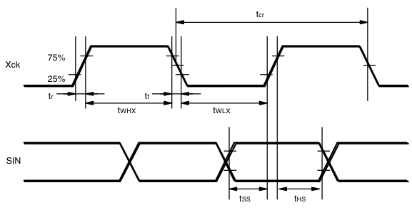
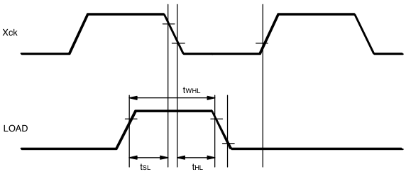
AC Timing Requirements
See the waveforms.
| Symbol | Parameter | Limits | Unit | ||
|---|---|---|---|---|---|
| Min. | Typ. | Max. | |||
| tcr | Xck cycle time | 2 | — | — | µs |
| tWHX | Xck high pulse width | 0.8 | — | — | µs |
| tWLX | Xck low pulse width | 0.8 | — | — | µs |
| tr | Xck rise time | — | — | 0.2 | µs |
| tf | Xck fall time | — | — | 0.2 | µs |
| tSS | SIN setup time | 0.4 | — | — | µs |
| tHS | SIN hold time | 0.4 | — | — | µs |
| tSL | SIN setup time | 0.4 | — | — | µs |
| tHL | SIN hold time | 0.4 | — | tWLX - 0.4 | µs |
| tWHL | LOAD high pulse width | 0.8 | — | — | µs |
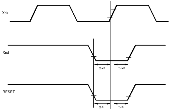
| tSXR | Xrst setup time | 0.4 | — | — | µs |
| tHXR | Xrst hold time | 0.4 | — | — | µs |
| tSR | RESET setup time | 0.4 | — | — | µs |
| tHR | RESET hold time | 0.4 | — | — | µs |
Xck, SIN timing
xck LOAD timing
Xck, Xrst, RESET timing
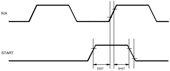
Xck, START timing
Operation
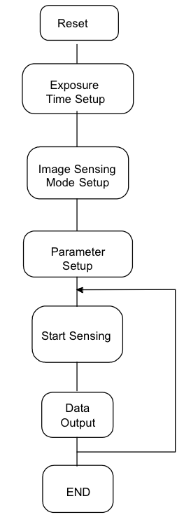
Figure 11-1 shows the image sensing sequence. First of all, all the registers must be reset and must be initialized to the appropriate values. The reset sequence completes when both Xrst and RESET signals are set low. There are 8 sets of registers, each of which consists of 8 bits of data. Each input data consists of 11 bits; of these 11 bits, the first 3 bits are the address and the last 8 bits are the data. The input data is latched at the rising edge of Xck when LOAD signal is high, and the data of a register become valid at the falling edge of Xck.
After all register are set, START signal must be asserted. Then, image sensing sequence starts at the rising edge of Xck. Image sensing sequence consists of two different processes: the exposing process to adjust the light intensity and the image read process to put out the image data after converting optical signal into electrical signal. After the exposure time defined by the registers 2 and 3 has passed, analog image data (total 16k pixels) is read out. To read image signal, READ signal must be asserted. At this moment, it becomes possible to change the registers, because the registers are irrelevant to the image read sequence.
Once image sensing sequence starts, the chip will continue to put out image data until it is reset.
Parameter Register Assignments
| Symbol | Bit Assignment | Operation |
|---|---|---|
| N | 1 bit | Exclusively set edge enhancement mode |
| VH | 2 bits | Select vertical - horizontal edge operation mode |
| E | 4 bits | Edge enhancement ratio |
| Z | 2 bits | Zero point calibration ( Set the dark level output signal to Vref ) |
| I | 1 bit | Select inverted/non-inverted output |
| C0, C1 | 8 bits x 2 | Exposure time |
| O | 6 bits | Output reference voltage ( In both plus and minus direction ) |
| V | 3 bits | Output node bias voltage (Vref) |
| G | 5 bits | Analog output gain |
| P, M, X | 8 bits x 3 | 1-D filtering kernel. |
Image Acquisition Modes
| (a) | Positive Image | Set “P” register |
| (b) | Negative Image 1 | Set “I” register |
| (c) | Negative Image 2 | Set “M” register (optional) |
| (d) | Edge Extraction (V, H, 2-D) | Set “N” and “VH” register |
| (e) | Edge Extraction (1-D) | Set “P” and “M” register (optional) |
| (f) | Edge Enhancement | Set “N”, “VH” and “E” register |
| (g) | Offset Level Output | Set “0” to both “C0” and “C1” |
Register Assignment
| Reg.No. | Address | 7 | 6 | 5 | 4 | 3 | 2 | 1 | 0 |
|---|---|---|---|---|---|---|---|---|---|
| 1 | 001 | N | VH1 | VH0 | G4 | G3 | G2 | G1 | G0 |
| 2 | 010 | C17 | C16 | C15 | C14 | C13 | C12 | C11 | C10 |
| 3 | 011 | C07 | C06 | C05 | C04 | C03 | C02 | C01 | C00 |
| 4 | 100 | P7 | P6 | P5 | P4 | P3 | P2 | P1 | P0 |
| 5 | 101 | M7 | M6 | M5 | M4 | M3 | M2 | M1 | M0 |
| 6 | 110 | X7 | X6 | X5 | X4 | X3 | X2 | X1 | X0 |
| 7 | 111 | E3 | E2 | E1 | E0 | I | V2 | V1 | V0 |
| 0 | 000 | Z1 | Z0 | O5 | O4 | O3 | O2 | O1 | O0 |
Data LOAD sequence
About the image processing functions
Artificial retina chip can put out positive, negative, edge extracted, and edge enhanced image in accordance with the parameter register settings.
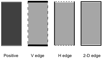
On-chip image processing is done with the 3 x 3 neighboring pixels. This chip executes subtraction between the central pixel P and the four neighboring pixels MN, MS, MW, and ME(see the right figure) to realize edge extraction as shown below: vertical edge (V edge), horizontal edge (H edge), and 2 dimensional edge (2-D edge). Moreover, this chip can program the weight value of the central pixel P and the other four pixels to produce edge enhanced images.
| Edge Modes | Output Signal | Effective Pixels |
|---|---|---|
| V-Edge Extraction | {2P - (MN+MS)} x α P-MS | 128(H) x 121(V) 128(H) x 123(V) |
| H-Edge Extraction | {2P - (MW+ME)} x α | 128(H) x 123(V) |
| 2D-Edge Extraction | {4P - (MN+MS+ME+MW)} x α | 128(H) x 121(V) |
| V-Edge Enhancement | P + {2P - (MN+MS)} x α | 128(H) x 121(V) |
| H-Edge Enhancement | P + {2P - (MW+ME)} x α | 128(H) x 123(V) |
| 2D-Edge Enhancement | P+{4P - (MN+MS+ ME+ MW)} x α | 128(H) x 121(V) |
α is the edge enhancement ratio set by “E” register. P and M indicate the signal value from each pixel.
