DMG Schematics
From GbdevWiki
See also SGB Schematic.
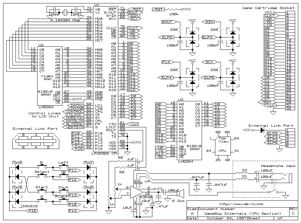
CPU Board
This schematic includes:
- LR35902, The main CPU (Commonly known as GB-Z80; with pinout)
- LH5264, 8192 byte work RAM (With pinout)
- LH5264, 8192 byte video RAM (With pinout)
- External Link Port (With pinout)
- Game Cartridge Socket (With pinout)
- Joypad Matrix (D-pad: Left, right, up, down. Buttons: B, A, Start, Select)
- Audio Amplifier
- Headphone Jack Daughter Board
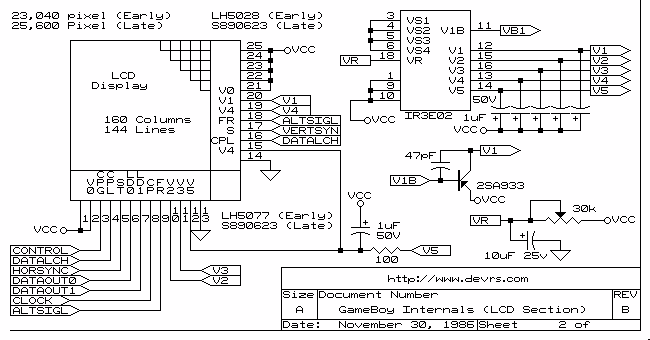
Display
This schematic includes:
- LH5028/LH5077 (Early screen model, 23040 pixels; with pinout)
- S890623 (Late screen model, 25600 pixels; with pinout)
- IR3E02 (With pinout)
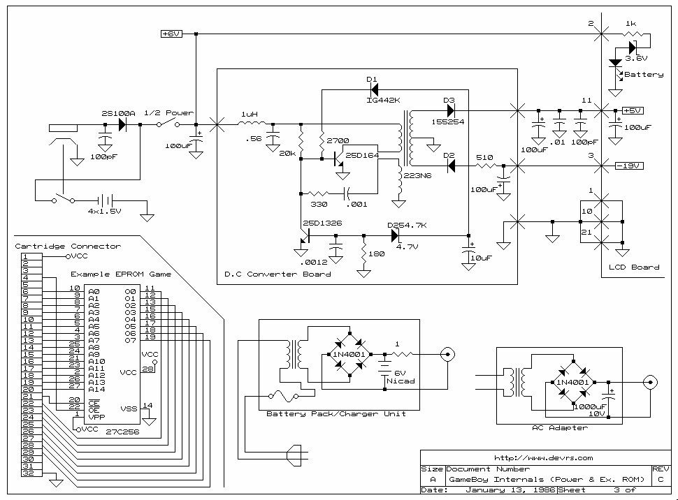
Switching Power Supply
This schematic includes:
- DC Converter Daughter Board
- Input: +6 V (Battery or mains)
- Output: +5 V (Logic) and -19 V (LCD)
- Example EPROM Game
- Battery Pack/Charger Unit
- AC Adapter
Source
Source: http://www.devrs.com/gb/hardware.php#hardgb (c) Jeff Frohwein


