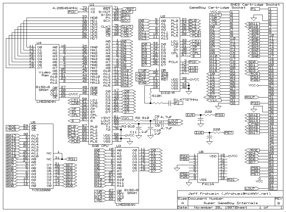
SGB Schematic
From GbdevWiki
Revision as of 21:17, 9 March 2008 by Nitro2k01 (Talk | contribs) (New page: == Super Gameboy Schematic == Image:Super-gameboy.gif This schematic includes: * SGB CPU (With pinout) * LH52A64N, 8192 byte work RAM (With pinout) * LH52A64N, 8192 byte video RAM (W...)
Super Gameboy Schematic
This schematic includes:
- SGB CPU (With pinout)
- LH52A64N, 8192 byte work RAM (With pinout)
- LH52A64N, 8192 byte video RAM (With pinout)
- TC53200 and F411A (Probably the ROM chip for the snes software and a lockout chip, respectively)
- ICD2-R the bridge between the SGB CPU and the SNES. Handles video and key presses. More info wanted.
Hardware Level Backwards Compatibility
- The SuperGB main chip has the necessary pins for serial communication. Thus it is possible to add a link port to a Super Gameboy. Super Gameboy 2 was shipped with a link port.
- It is not known whether the Vin pin of the SGB CPU works as intended.
- What does the PX pin do? (Pin 53 of the CPU)
Source
(c) Jeff Frohwein Source: http://www.devrs.com/gb/hardware.php#hardgb
