MBC5
The copy of Pan Docs hosted on this wiki is considered deprecated.
Pan Docs is now officially hosted on gbdev.io as a living document. Please go to https://gbdev.io/pandocs/ to read Pan Docs or to https://github.com/gbdev/pandocs to contribute.
Click here to go to this section of Pan Docs in the new location: https://gbdev.io/pandocs/#memorybankcontrollers
Contents
- 1 Overview
- 1.1 0000-3FFF - ROM Bank 00 (Read Only)
- 1.2 4000-7FFF - ROM Bank 00-1FF (Read Only)
- 1.3 A000-BFFF - RAM Bank 00-0F, if any (Read/Write)
- 1.4 0000-1FFF - RAM Enable (Write Only)
- 1.5 2000-2FFF - Low 8 bits of ROM Bank Number (Write Only)
- 1.6 3000-3FFF - High bit of ROM Bank Number (Write Only)
- 1.7 4000-5FFF - RAM Bank Number (Write Only)
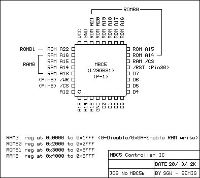
- 2 Schematic
Overview
MBC5 (Memory Bank Controller 5) is the 4th generation MBC. There apparently was no MBC4, presumably because of the superstition about the number 4 in Japanese culture. It is the first MBC that is guranteed to work properly with GBC double speed mode. It can map up to 64 Mbits (8 MBytes) of ROM.
0000-3FFF - ROM Bank 00 (Read Only)
Same as for MBC1.
4000-7FFF - ROM Bank 00-1FF (Read Only)
Same as for MBC1, except that accessing up to bank 1E0h is supported now. Also, bank 0 is actually bank 0.
A000-BFFF - RAM Bank 00-0F, if any (Read/Write)
Same as for MBC1, except RAM sizes are 64kbit, 256kbit and 1mbit.
0000-1FFF - RAM Enable (Write Only)
Mostly the same as for MBC1, a value of 0Ah will enable reading and writing to external RAM. A value of 00h will disable it.
2000-2FFF - Low 8 bits of ROM Bank Number (Write Only)
The lower 8 bits of the ROM bank number goes here. Writing 0 will indeed give bank 0 on MBC5, unlike other MBCs.
3000-3FFF - High bit of ROM Bank Number (Write Only)
The 9th bit of the ROM bank number goes here.
4000-5FFF - RAM Bank Number (Write Only)
As for the MBC1s RAM Banking Mode, writing a value in range for 00h-0Fh maps the corresponding external RAM Bank (if any) into memory at A000-BFFF.
Schematic
Source: [1]
